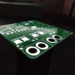


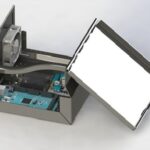
PCB Design & Fabrication
PCB Design Capabilities
Expertly engineered for HDMI, Ethernet, PCIe, USB, Thunderbolt, and other high-speed interfaces. We ensure signal integrity through impedance control, crosstalk mitigation, and matched routing strategies.
Sophisticated PDN (Power Delivery Network) design to ensure voltage stability, low noise, and robust decoupling. Our PI engineering supports high-performance digital systems with clean power delivery and reduced ripple.
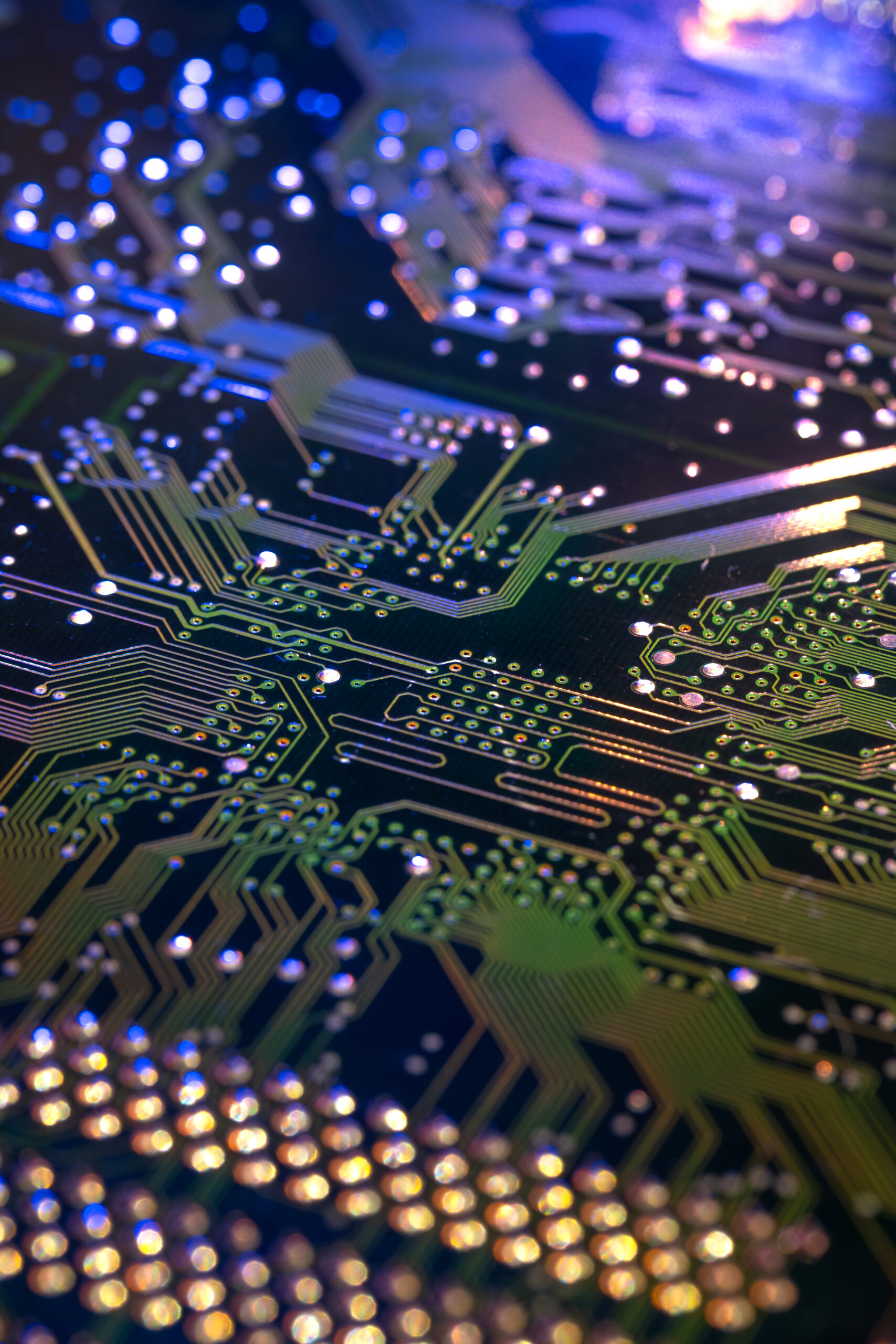
Expertise across rigid, flex, rigid-flex, HDI (High Density Interconnect), blind & buried vias, multi-layer stack-ups, and high-density layouts.
Strategic selection of materials such as FR-4, Rogers, Megtron, Taconic, and custom high-frequency laminates, optimized for signal and power performance.
We embed DFM, DFT, DFA, and DFC principles to minimize production costs and simplify assembly, all while maintaining optimal reliability.
Key Technical Capabilities
Tailored multi-layer designs with controlled impedance, split planes, and thermal considerations.
Precision-driven placement to minimize trace lengths, noise coupling, and optimize routing efficiency.
Advanced routing rules for equalized lengths, impedance consistent paths, and minimized via use for high-speed signal fidelity.
Integrated signal and power integrity simulation, EMI/EMC mitigation, and thermal modeling for robust designs.
BGA (including fine-line and micro‑BGA), 01005 discretes, mixed-signal ICs, custom power modules, and embedded components.